Autoliv NV2 Nightvision Camera teardown
TL;DR: 325x256 30fps Automotive Thermal Camera can be hacked to run on a Raspberry Pi+FPGA.
Hardware
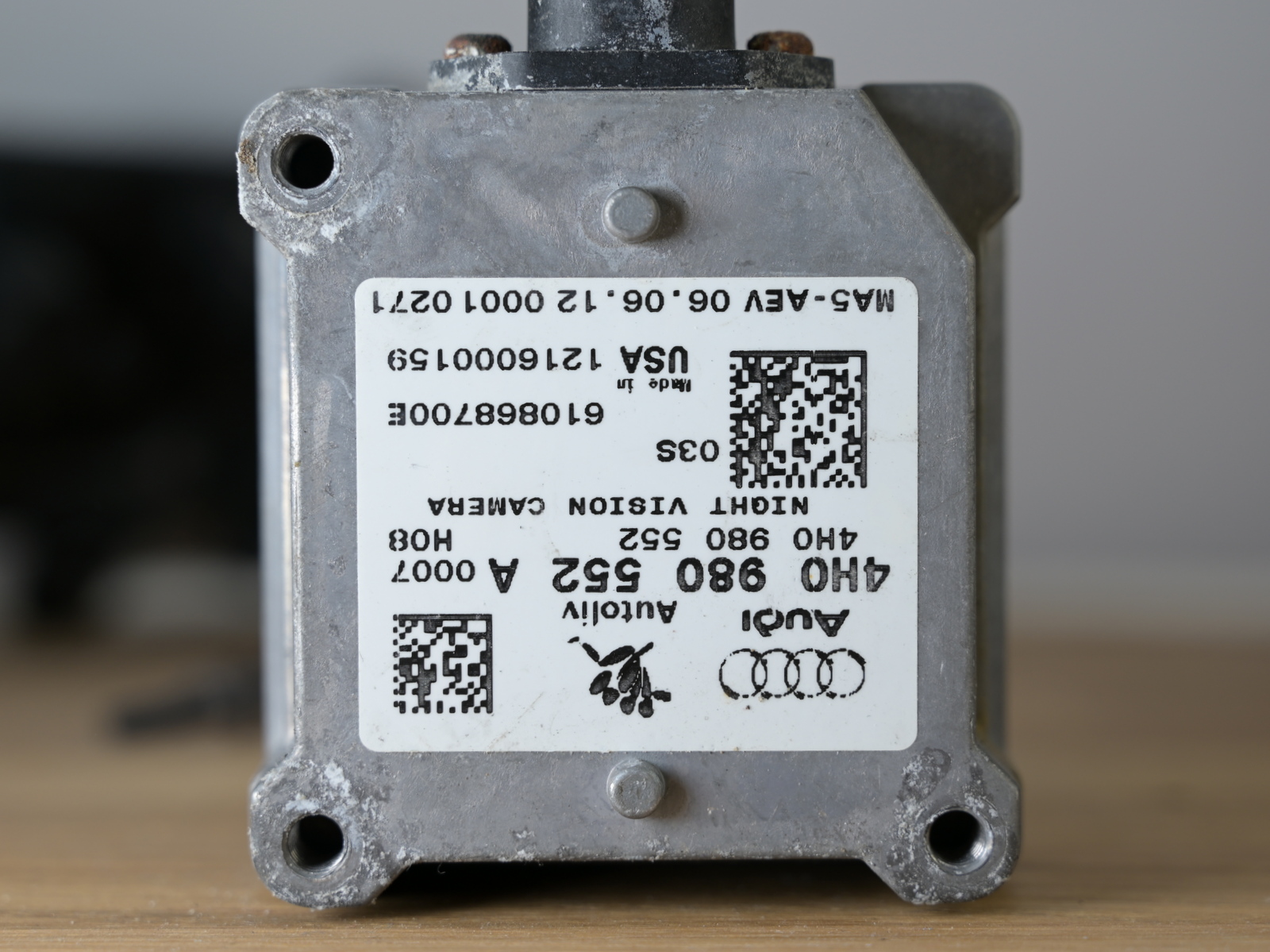
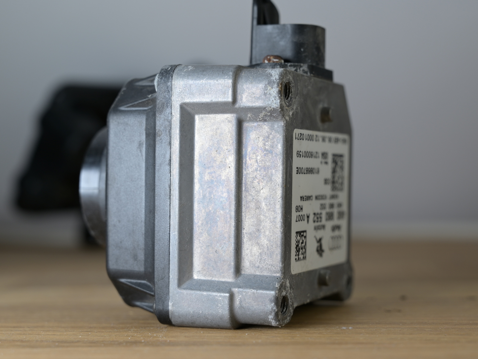
The Autoliv NV2 is a “passive Night Vision” camera, operating in the LWIR range. Mike did a teardown of it a few years back, which got me interested into this camera.
This particular camera was used until a few years ago in certain configurations of high-end Audi and BMW cars. (There’s a newer version - the NV3 - which is essential a cost reduction.)
There’s an interesting - unfortunately bad quality - official video that shows the features of this system, as well as some screenshots from a development system.
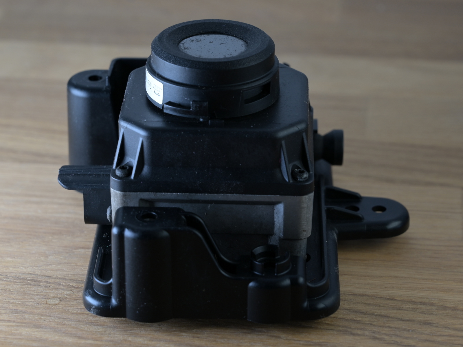
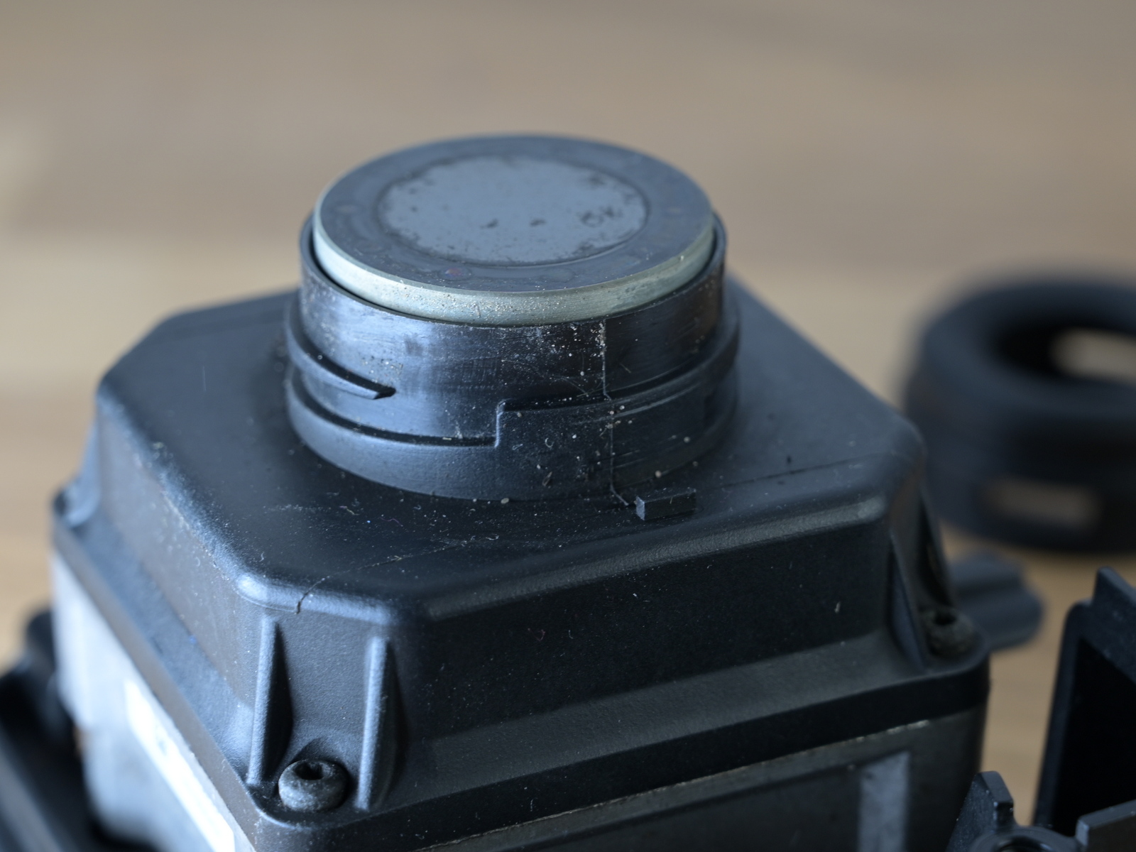
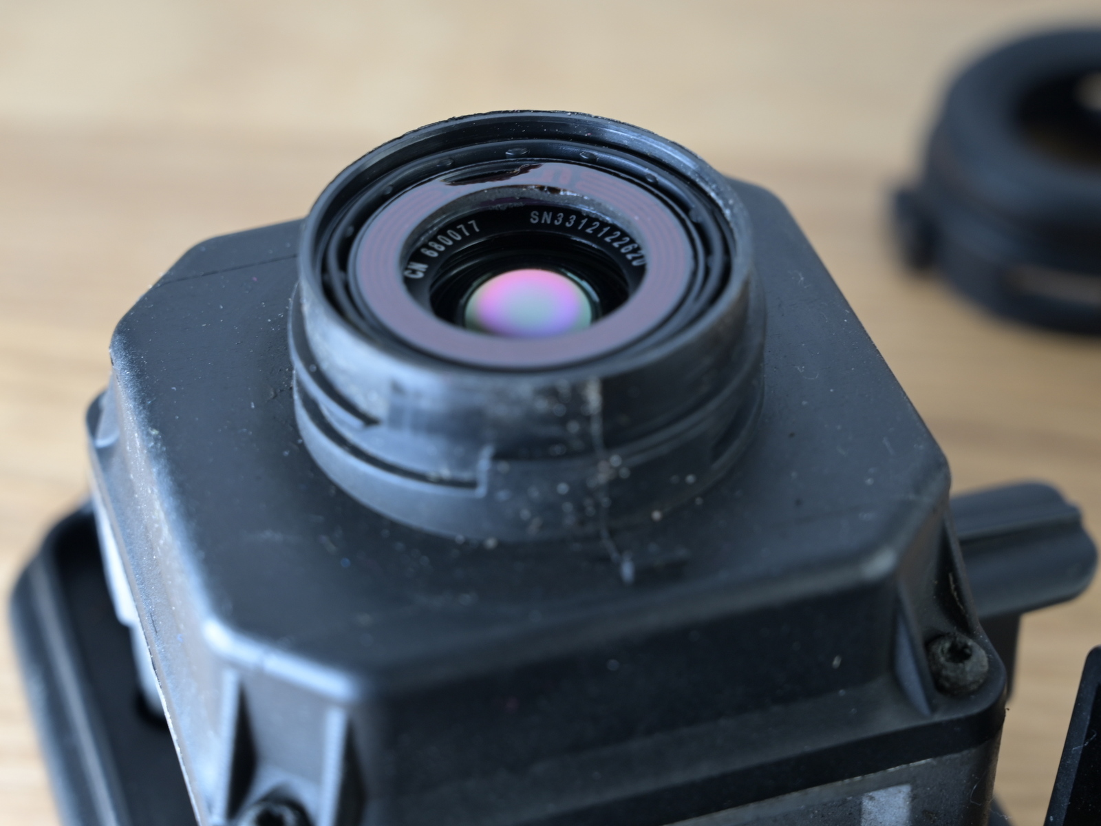
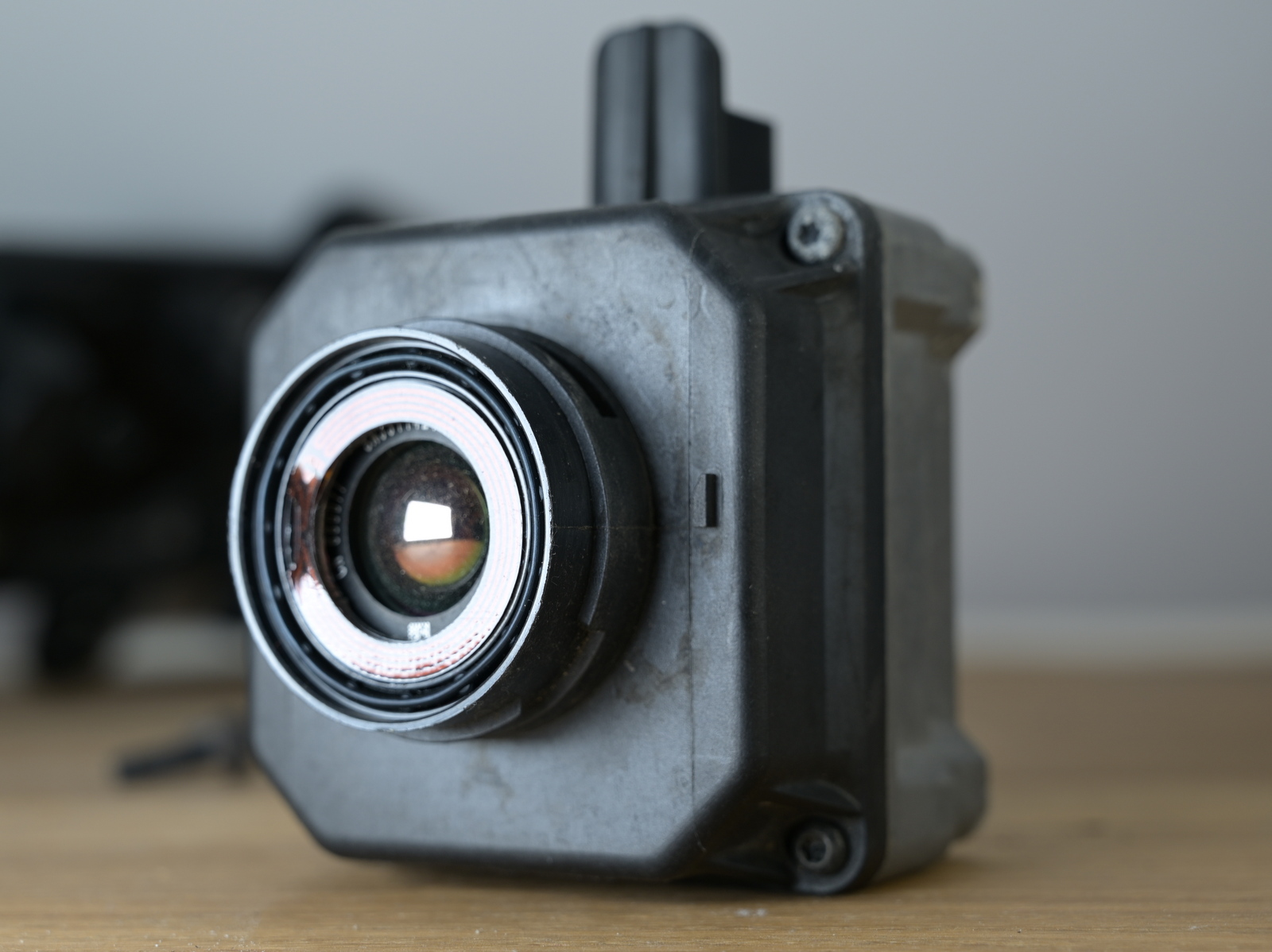
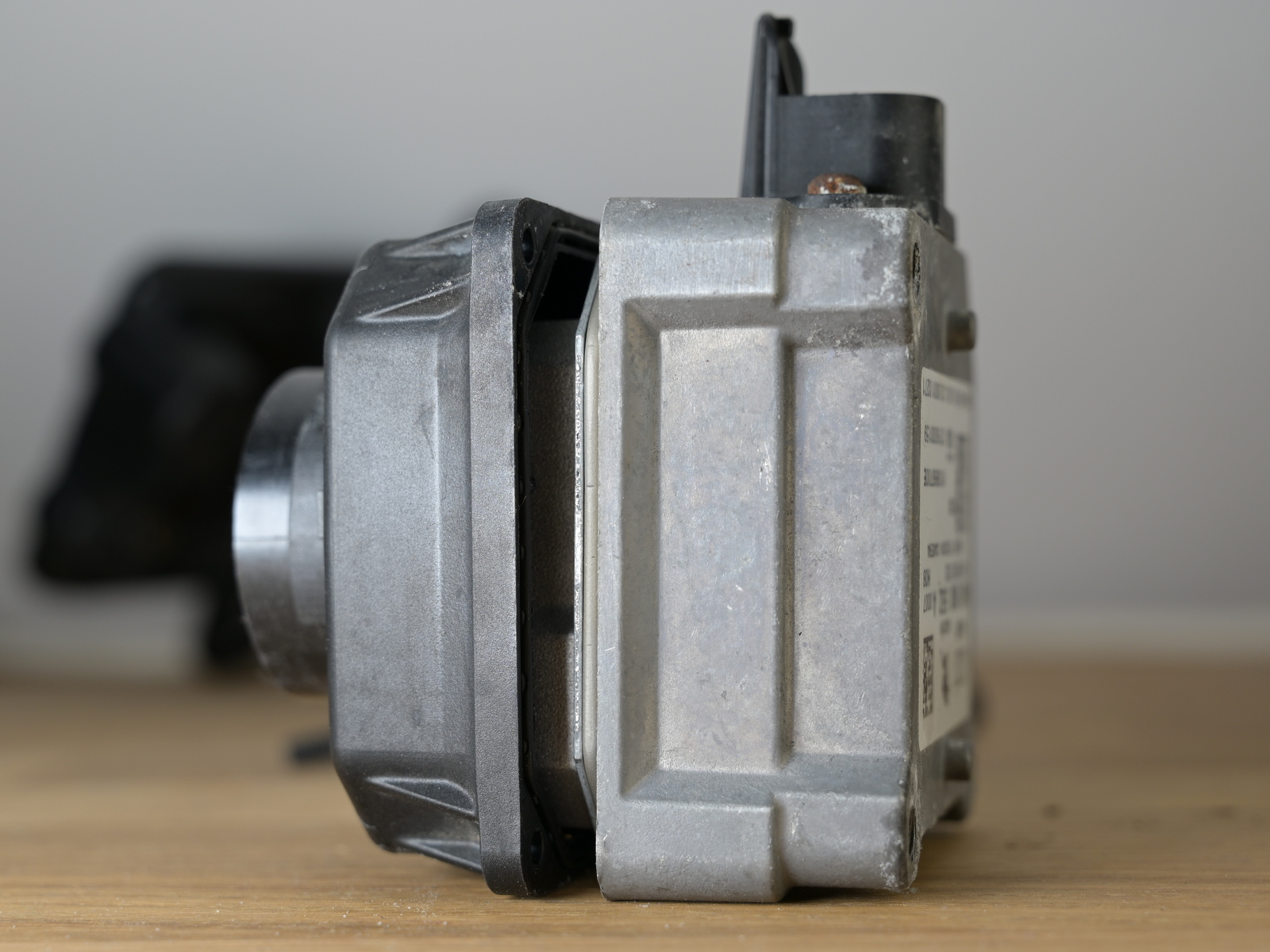
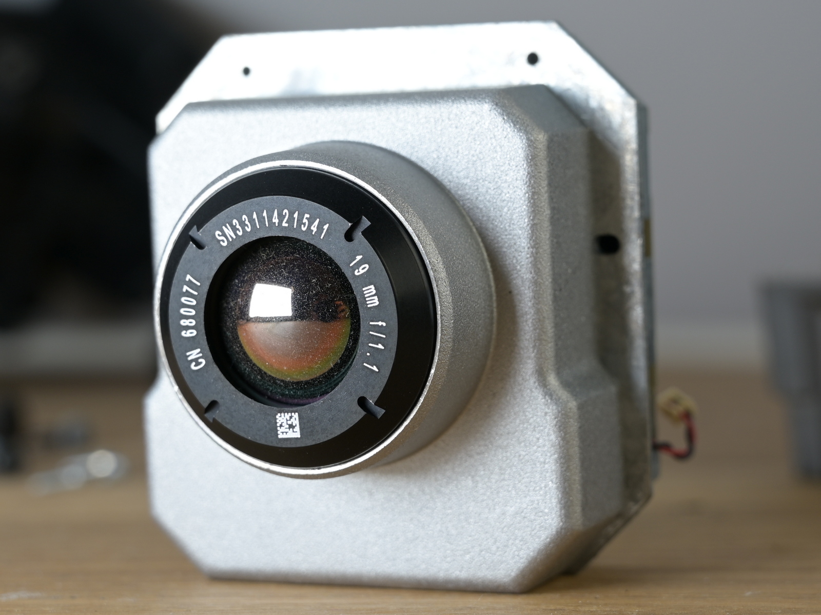
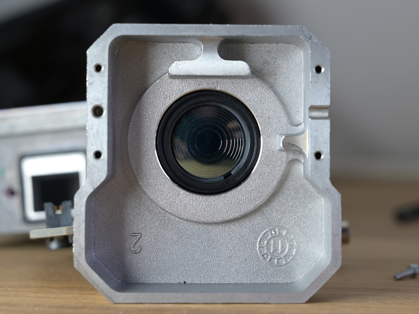
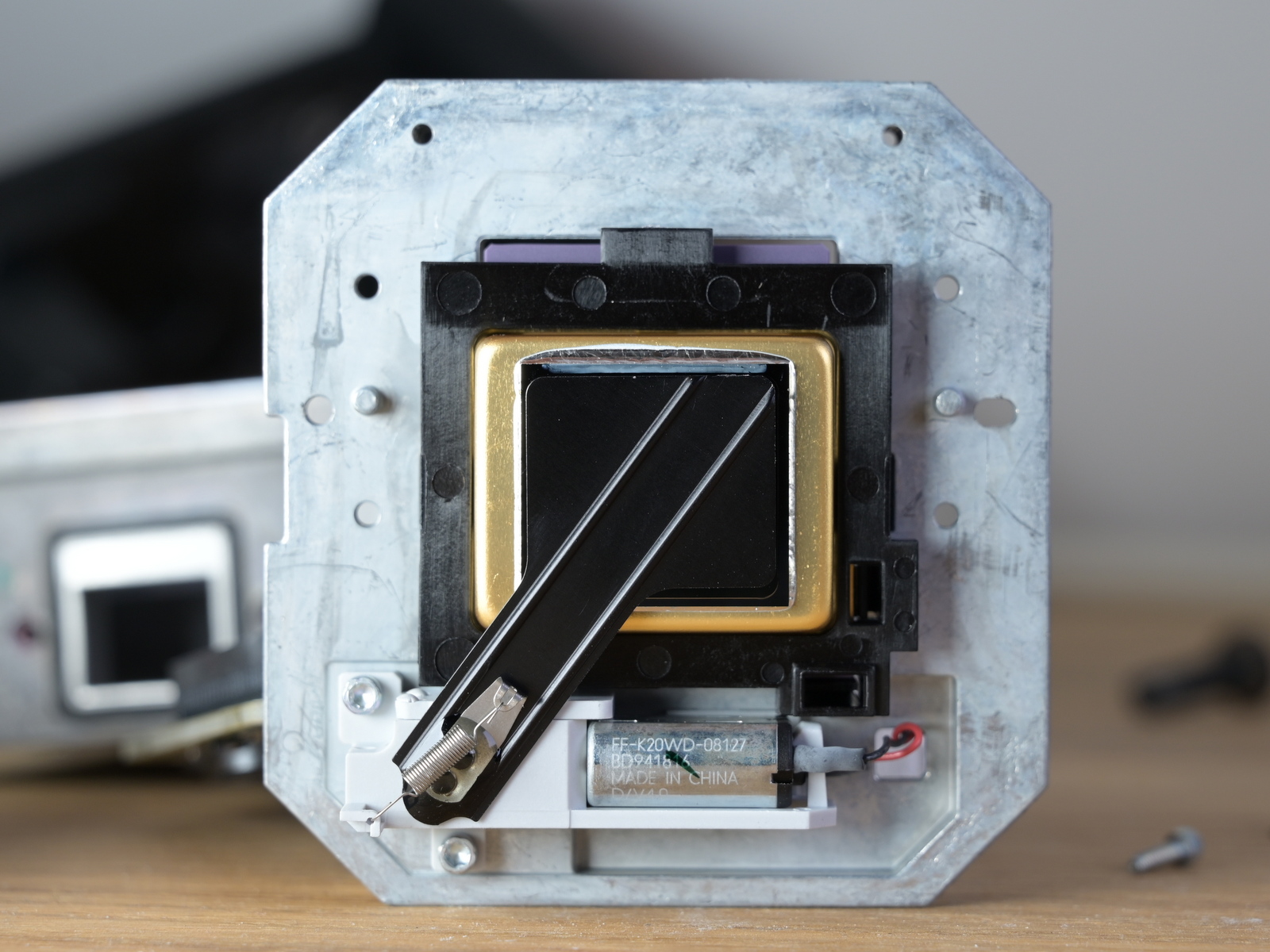
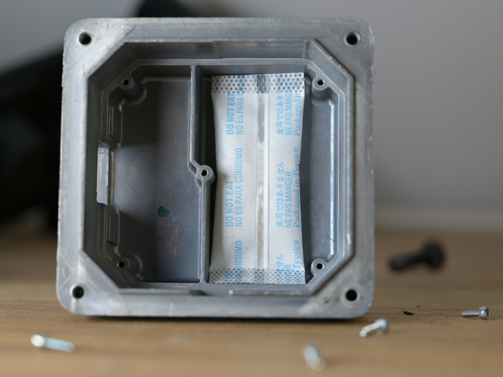
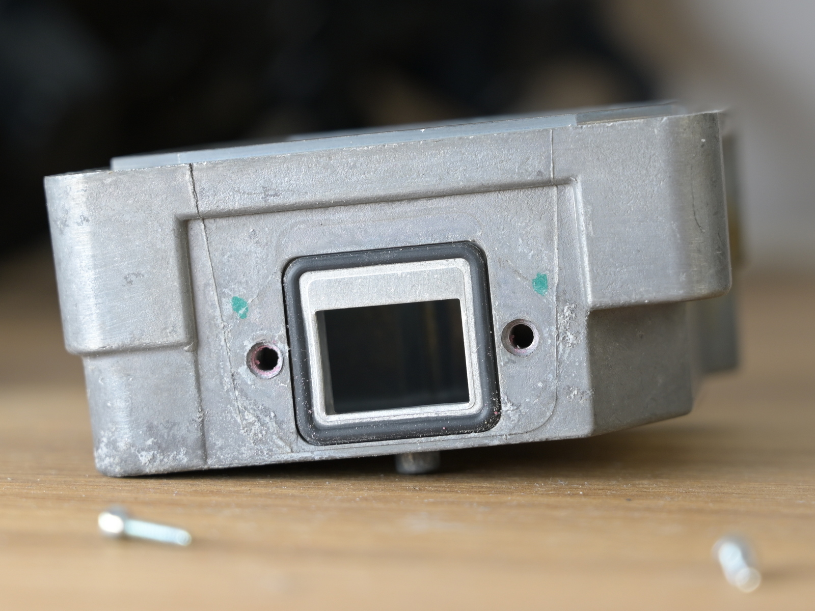
The night vision camera needs to be exposed directly to the weather outside. Because of that, there’s extensive water protection. This starts with a protective glass element, which is held in front of the actual lens. The cover can be removed - there’s even an official “repair kit” to replace the glass in case it gets chipped by a stone. The protective element can also be heated electrically. Underneath there is the the 19mm f/1.1 LWIR lens.
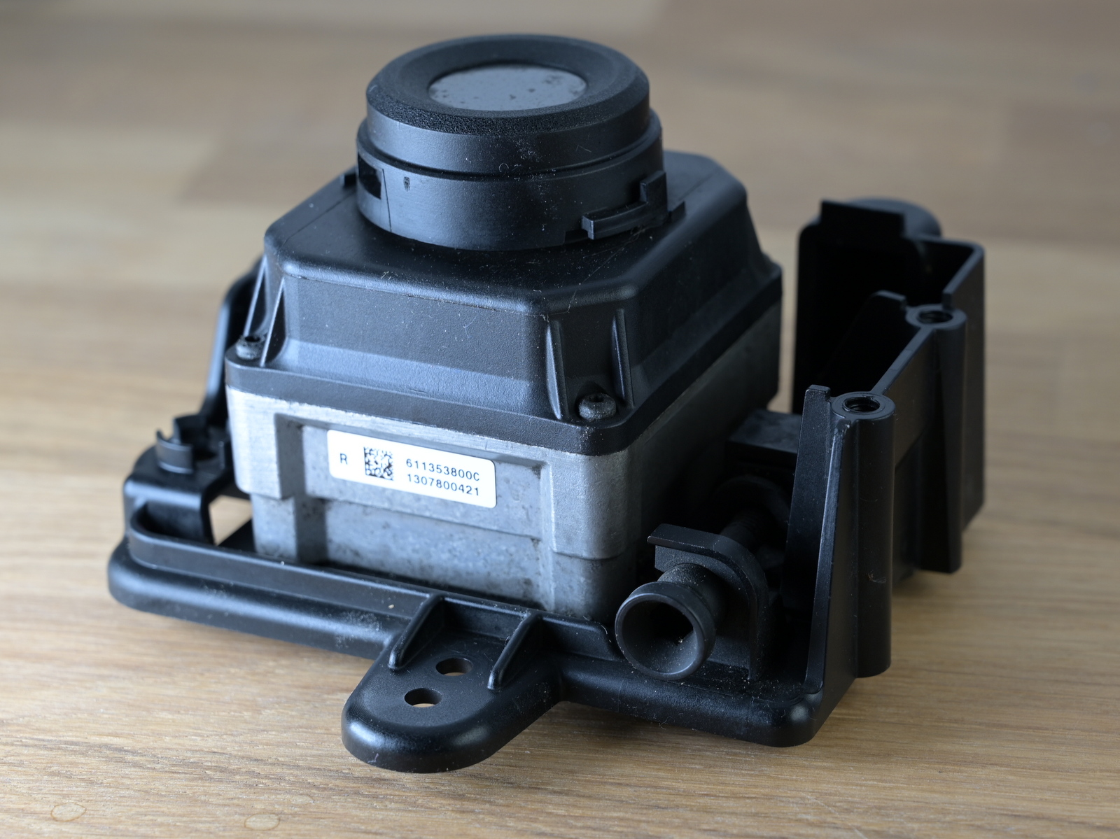
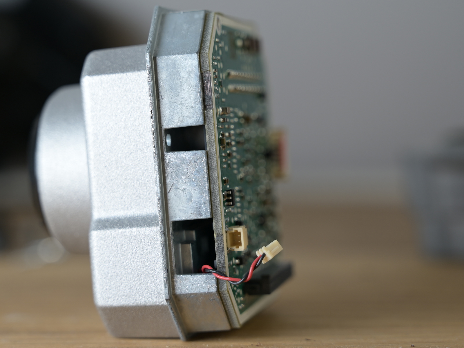
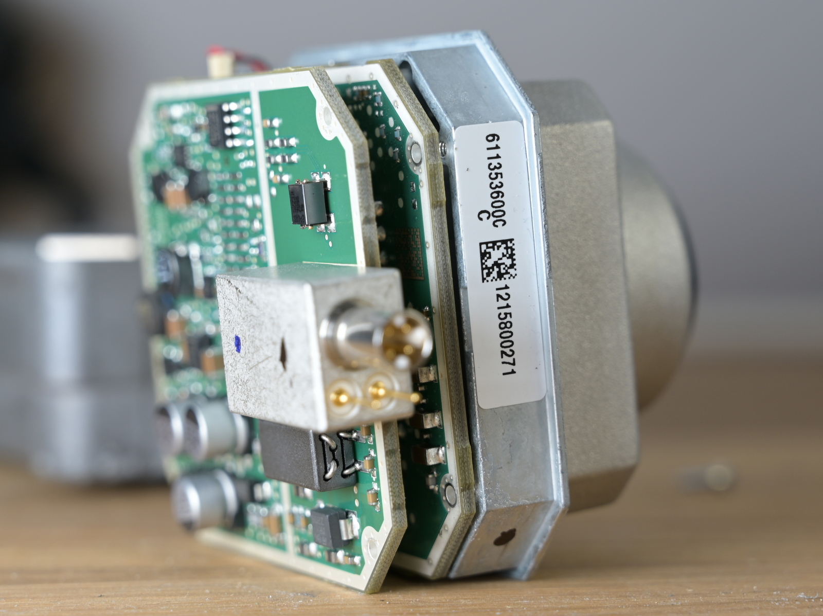
After removing the four outer screws, the plastic can be lifted. However the flex cable for the heating is still connected, and there’s risk in ripping it apart when pulling the plastic. Instead, the plastic front together with the metal case of the sensor can be grabbed. It detaches - it’s connected with a 1mm header to the power PCB.
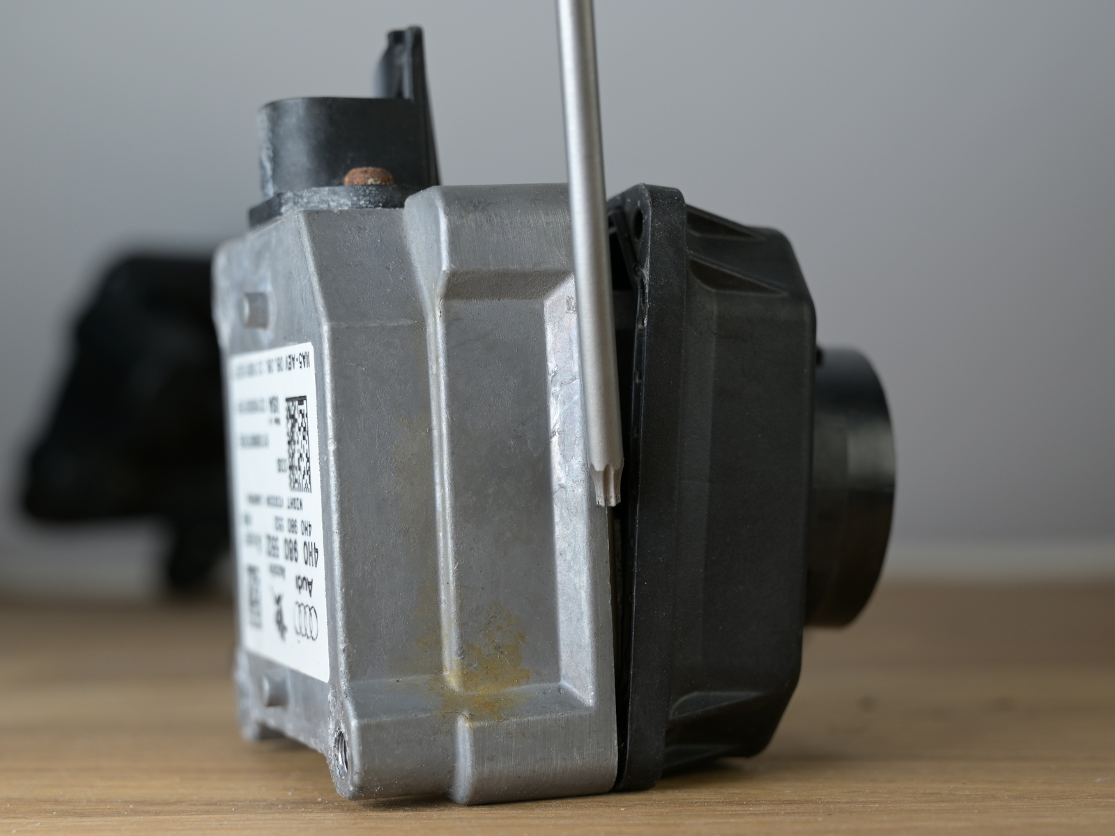
After that, the flex cable for the heatercan be removed, as well as the cable for the shutter. After that the video PCB can be removed.
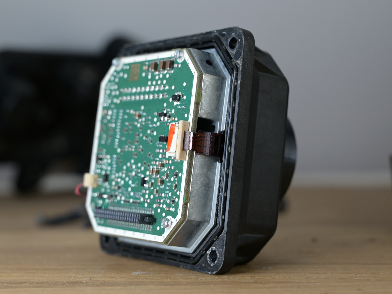
The sensor itself is a Flir ISC0601 (aka. SB320), a 324x256 25μm pitch, the same one as in the Flir E40 for example (though it’s crippled to quarter resolution there for product differentiation reasons). Little is publicly known about the interface to the sensor itself.
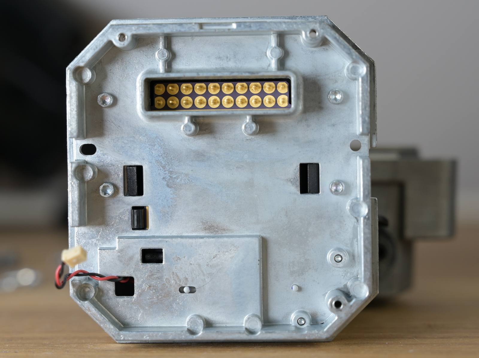
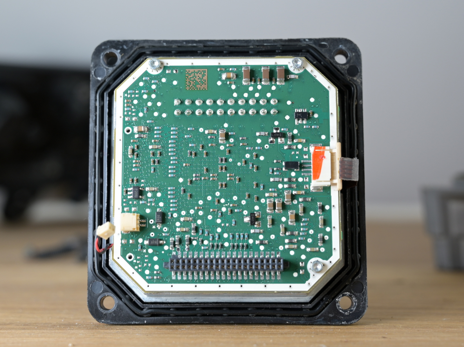
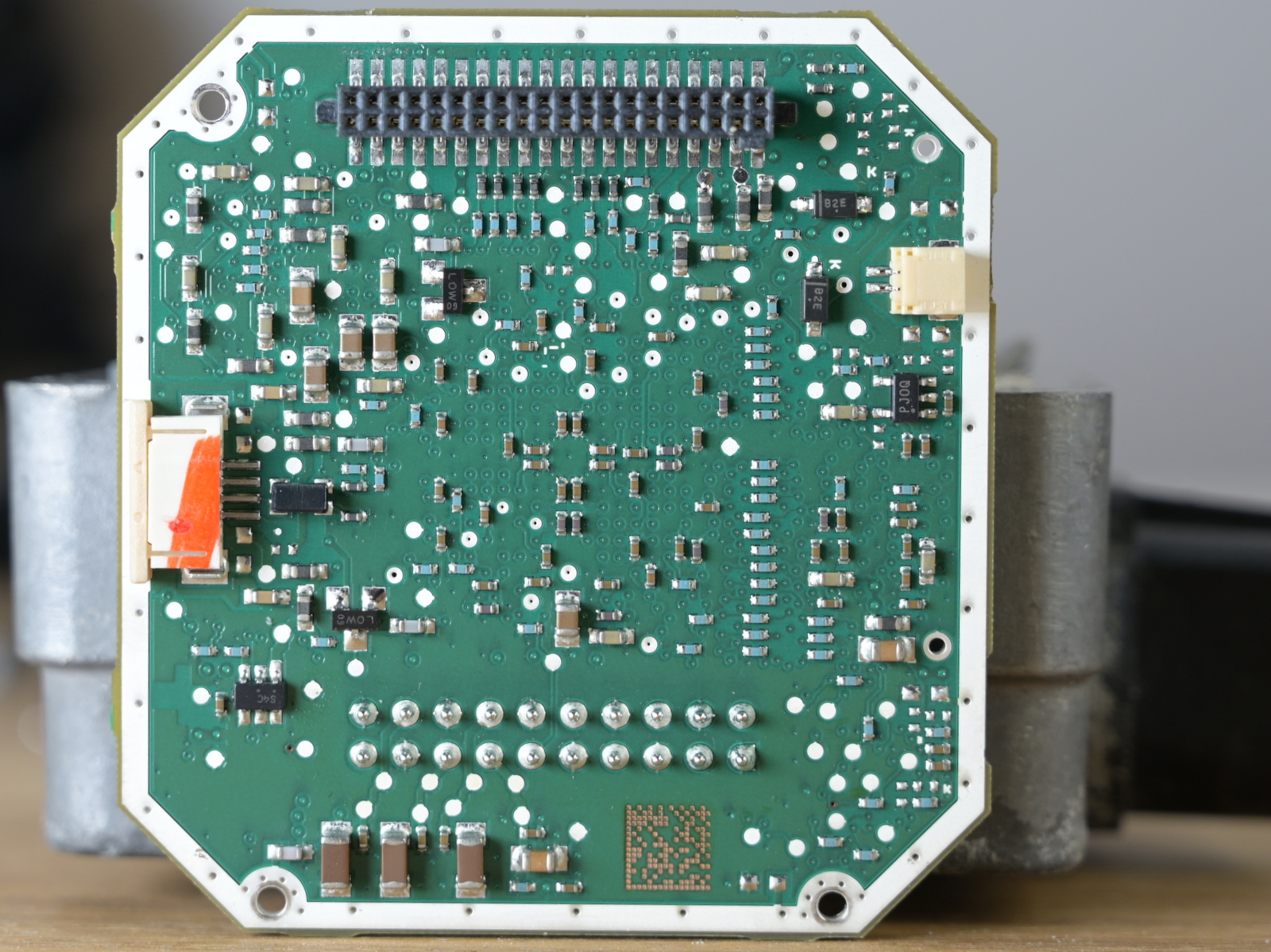
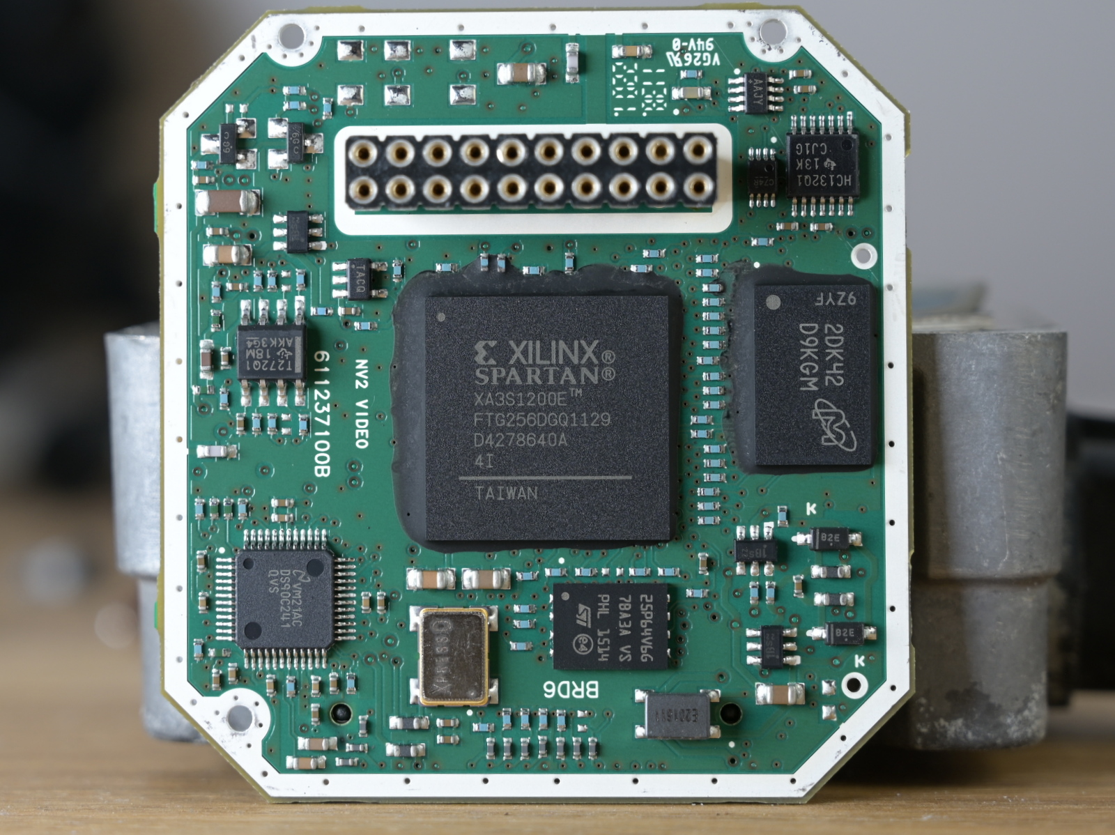
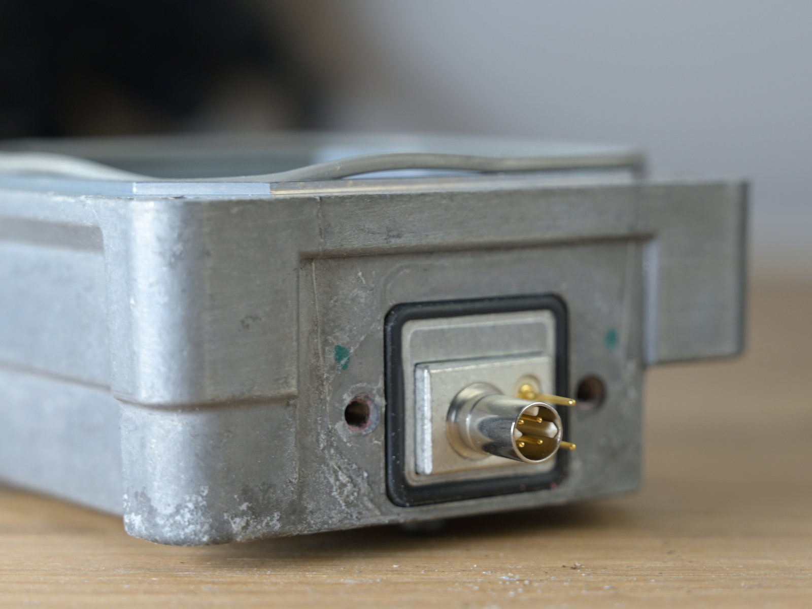
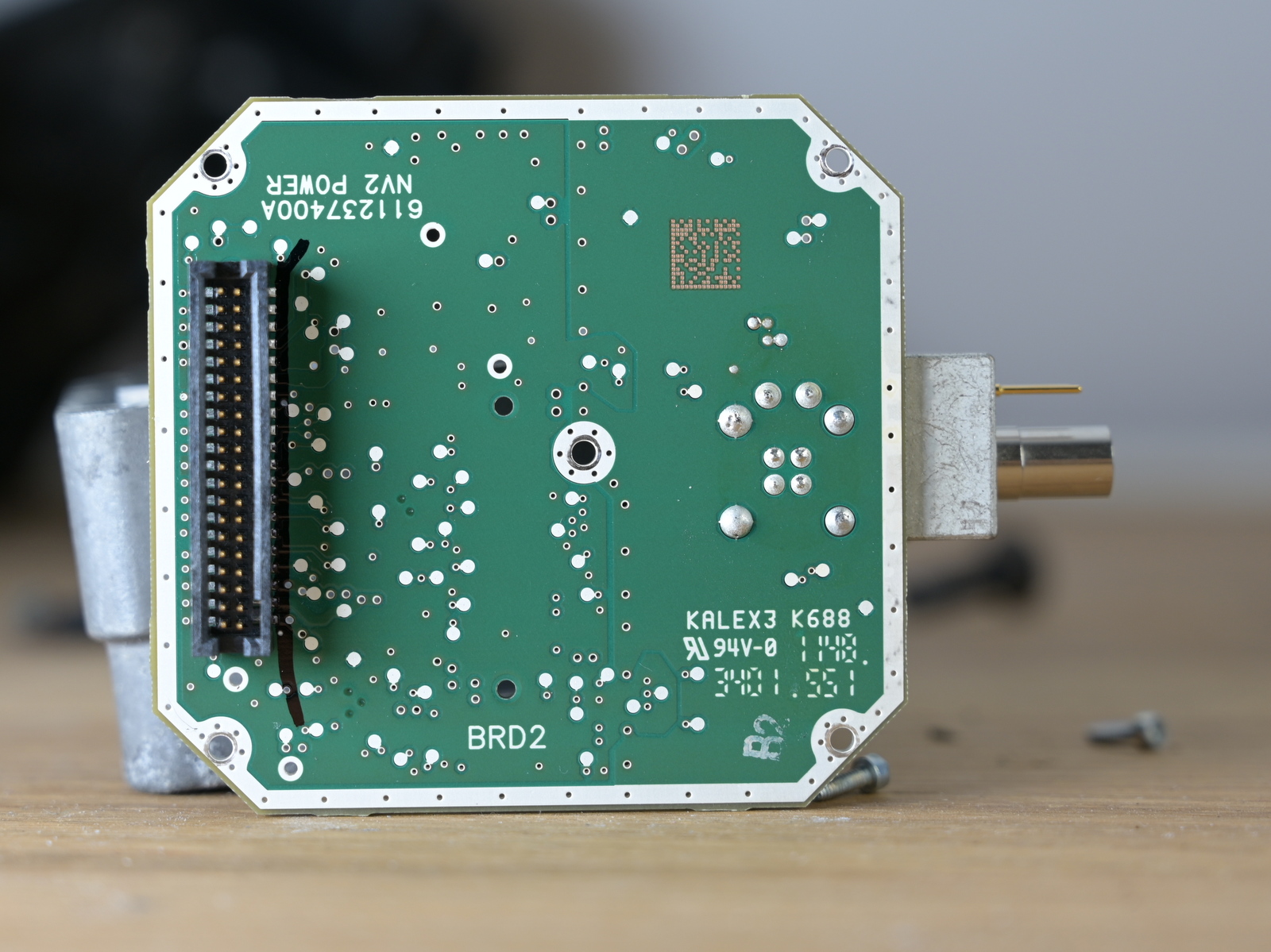
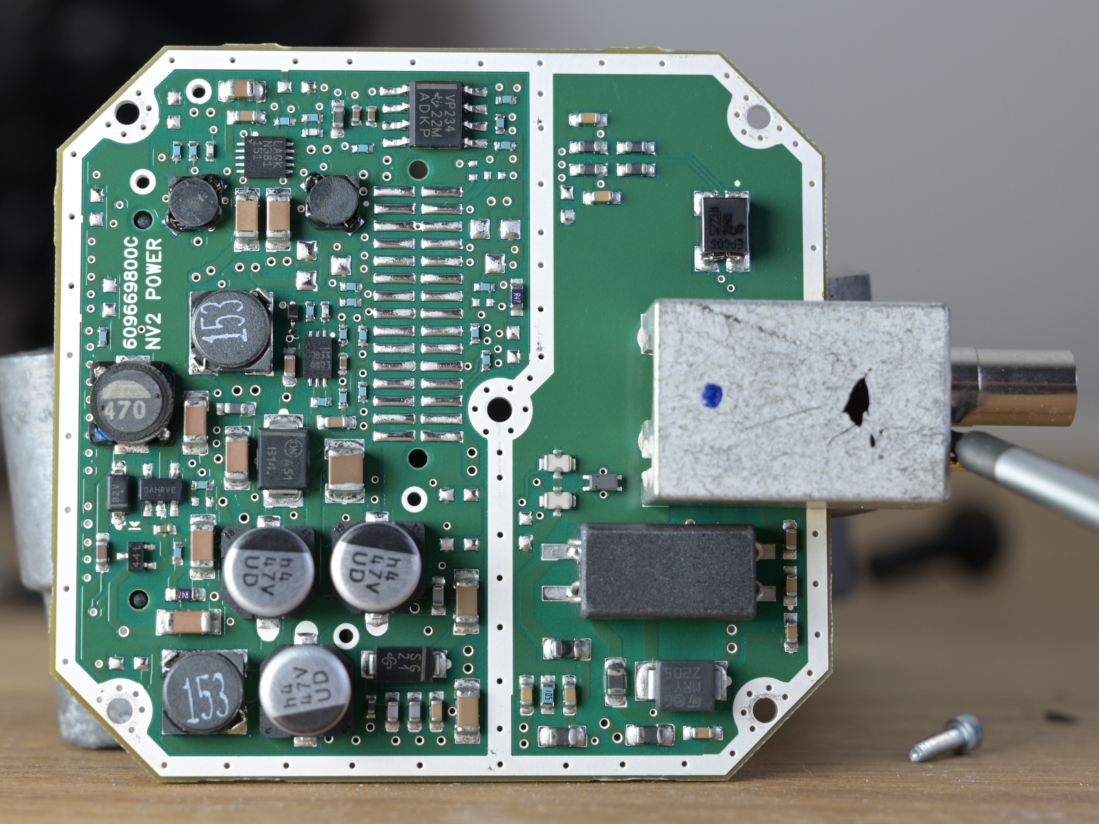
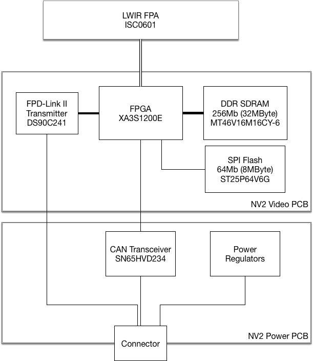
The PCB contains a Spartan XA3S1200E - the automotive version of well-known Spartan-3E - together with DDR SDRAM (32MBytes) and a SPI flash to boot from. The sensor is interfaced with a two-row .1” header, the connection to the power is via a two-rows 1mm header. The video board also contains an oscillator, and a National Semiconductor (now TI) DS90C124 FPD-Link II Serializer, which encodes 24-bit parallel data into a high(-ish) speed LVDS signal.
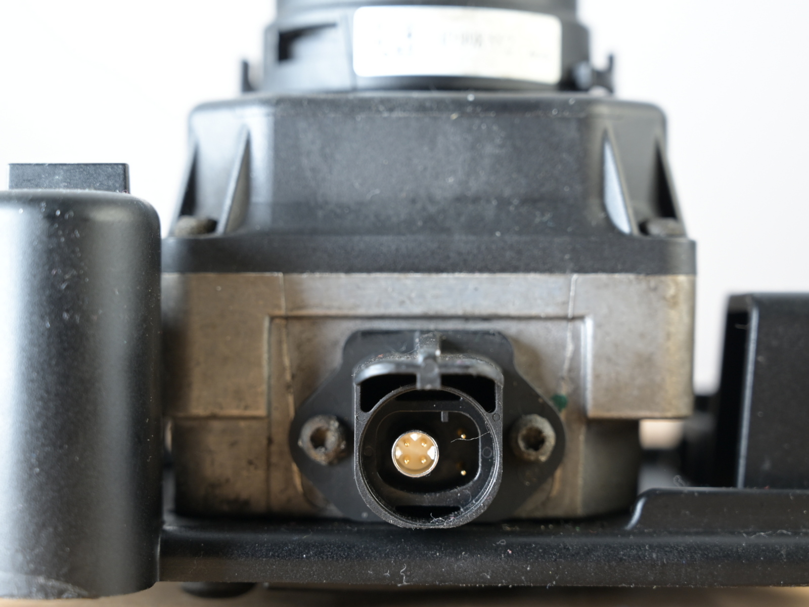
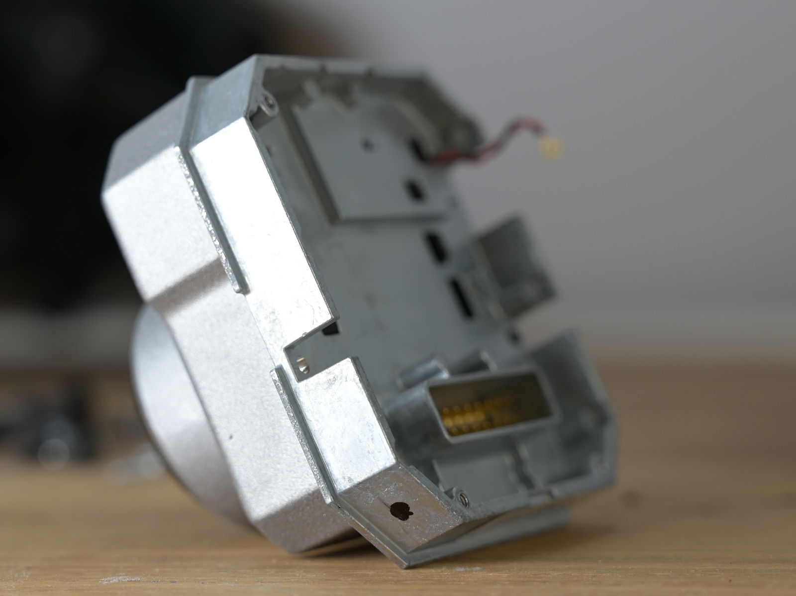
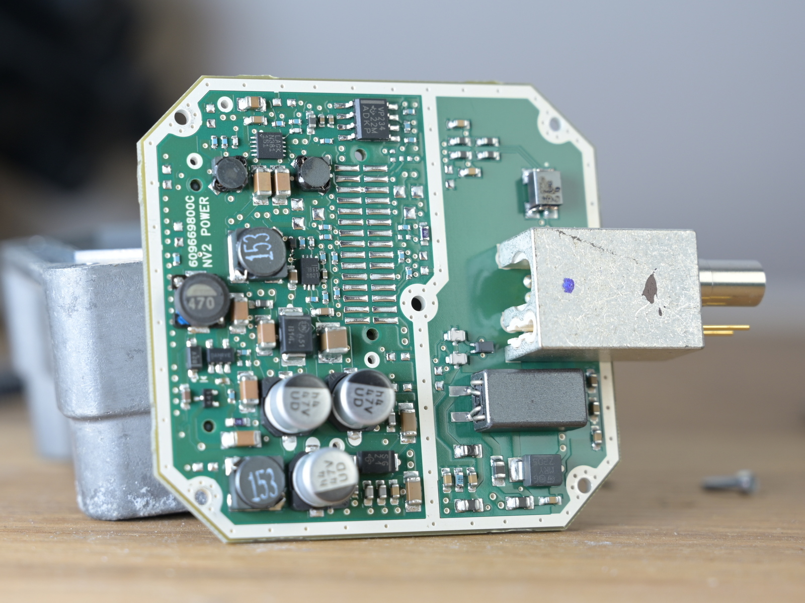
The power board can be removed from the back now by un-screwing the connector cap (and the PCB itself). Silica gel is used to remove residue moisture. Note the sealing around the connector.
Interfacing the Camera
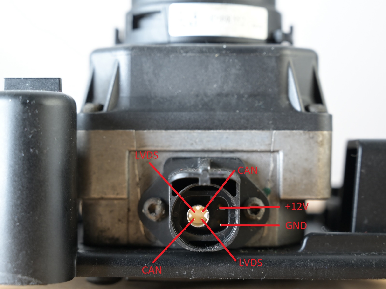
My goal was to interface the camera and obtain the thermographic image data. The first course of action is to apply power and see what happens. Unfortunately I did not have the original cable, so I just soldered wires to the pads on the power board.
The pinout is this:
- GND
- 12V
- CAN +/-
- LVDS +/-
When applying power, there’s a data signal on the LVDS bus. The DS90C124 on the video PCB is in charge of encoding the pixel data into an FPD-Link II stream, but when probing either the output of the encoder or the parallel input, it becomes clear that there is no useful data. There’s sync structure, and the data payload matches the expectations of the sensor readout speed, but all data is zero’ed.
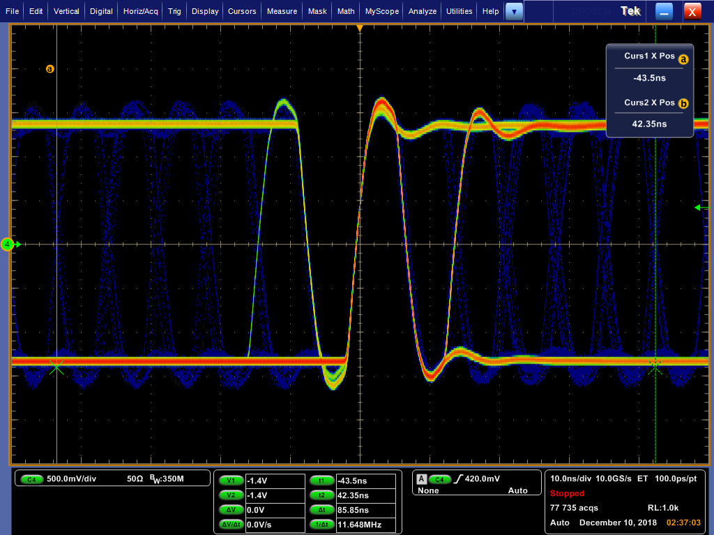
Here I’ve measured 12 UI as 85ns, resulting in a bitrate of 139.7 MBit/s (4.98 MPix/s; each FPD-Link II word is 28 bit). But it can also be seen that there isn’t a lot of entropy in the data - even though the scope captured 77k waveforms, only a handful of bit transitions outside of the middle were observed. This strongly indicates that there is no usable pixel data (yet).
Car Integration
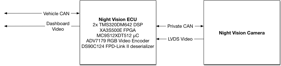
In the regular setup, a dedicated electronic control unit (ECU) receives the pixel data, does video processing on it (finding pedestrians etc.), and then outputs a video stream to be displayed on the vehicle’s head unit. At the same time, information is received from the vehicle’s CAN bus which is necessary for computing the expected trajectory - current speed, angular velocity etc. - in order to allow the ECU to give an audiovisual warning if the vehicle is steering into a human or animal. Finally, a PAL RGB picture is generated using a video encoder. This is done in two TMS320DM642 DSPs and a Spartan-3E 500.
The CAN bus of the camera itself is not connected to the vehicle’s CAN bus - it’s a private CAN bus just beween the ECU and the camera. Unfortunately I didn’t have a log of the communication on this bus. The expectation was that there’s some kind of an unlocking sequence required to enable the camera to send out real pixels.
My focus was to get the camera to work stand-alone (potentially to use it as a Night-Vision camera in my car, for which no Night-Vision option exists), which clearly it isn’t doing by default - the video data, as described above, is all-zero.
Software
The FPGA is configured with a SPI flash. Running strings on the dump discovers a few texts:
loadNUCToBuffer(%d->%d) @%u
Load NUC coeff Unity @%u
LoadBoloComp(%u) @%u
start readNUCDataTask=%d
end readNUCDataTask @%u
calcGainData done @%u
Copying simulated FPA image %d
Now, this is interesting. This isn’t part of the bitstream to configure the FPGA, as bitstreams - even when the included blockram initialization data contains strings - are not yielding plaintext strings. Further, the strings are found at the end of the flash image, and not the beginning (where the bitstream is located). Something is loading this code.
Looking at this in more details uncovers that there is something that looks like plaintext executable code. Let’s throw it into a disassembler! As this is an FPGA, and there doesn’t seem to be a separate microprocessor, it’s very likely that a soft core is used. Many soft cores are available, including 8-bit CPUs (shudder), so let’s hope it’s not that.
But which architecture? Trying the usual suspects (Z80, 8051, maybe ARM - though unlikely on a FPGA of that generation) ones doesn’t yield anything .
CPU Rec (cpu_rec is a tool that recognizes cpu instructions in an arbitrary binary file) to the rescue!
$ python3 cpu_rec.py code.bin
code.bin        full(0x20000)  None    chunk(0xe800;29)    MicroBlaze
MicroBlaze, sigh. Ok, we should have expected this, as MicroBlaze is/was the vendor-supported soft core for Xilinx FPGAs. There’s no IDA plugin for MicroBlaze (edit: I finally found one. I blame my search-skills. In retrospect I feel very stupid. Sorry about this!). So I wrote one (that has a few limitations, but worked well enough for this purpose).
MicroBlaze is a very simple, RISC CPU with only a handful of instructions. It uses delay slots, but otherwise it’s very similar to other architectures.
Observations
There appears to be some kind of a debug UART, at least there are a couple of places where debug strings are output. From that, basic functionality can be figured out. In the software, there is the CAN protocol handling. The hardware CAN registers match those of the Xilinx CAN Core, so it’s a good bet that they just used the Xilinx reference CAN IP.
In the automotive world, there’s a distinct pattern of CAN communication:
There’s functional communication, usually over small (<=8 bytes) packets that are just send periodically as CAN packets. There’s no standard about the meaning of the individual bits or allocation of CAN identifiers. By disassembling, it can be found out that the camera receives packets on IDs 401 and sends on 301, 302, 303 and 304, or 311, 312 and 313. This can be configured in the camera settings, but my camera was configured to use 301, 302, 303, 304. It’s also possible to query to camera by either sending a RTR packet or by sending a packet to ID 5D7. By sending various packets, I was able to control the camera heater and the shutter, but whatever I’d do, it would never send valid video data.
Then there’s diagnostic communication, which is standardized to a certain point. The NV2 implements UDS, “Unified Diagnostic Services” over ISO-TP on ID 657, extended address 8B. This allows for basic communication, reading out a few identifiers. It also allows for - vendor specific - access to RAM, Flash, writing calibration data etc., but most of this functionality is only available after a challege/response-based security challenge. The challenge/response protocol itself is defined in UDS (SID $27 - Security Access), but of course the actual algorithm is device-specific and usually secret.
Also there appears to be a serial command handling, but it doesn’t fundamentally offer different functionality than what is offered over the CAN diagnostic interface.
A Clue
But more importantly, the main loop appears to wait for a certain bit to be cleared. Only after that bit is cleared it will proceed further into a function that initializes the NUC (non-uniformity correction) and other things. Before, it merely listens to CAN messages.
Backtracing reveals that it only way to clear this bit appears to be the UDS security challenge. This gives a first lead - maybe the UDS security access needs to be completed to enable a picture. This is quite uncommon - for any other car ECU that I’ve looked at, functionality doesn’t depend on the diagnostic communication, but as this component is part of a private CAN network, eveyrthing is possible.
Let’s try to answer the challenge and see what happens. (Worst case we can then use then-unlocked memory read/write functions and get code execution).
A Key
Analysis shows that the challenge/response is an MD5-HMAC where the data is 12-byte random plus 4-byte serial number, and the key is stored in a static location in blockram. Because we don’t have code execution, we can’t dump that blockram. Because we don’t know the key, we can’t unlock the functions that would allow us to get code execution (or arbitrary memory reads).
What populates the blockram? It could be anything in the FPGA logic, but the default way to bootstrap a MicroBlaze is to put a small bootloader into blockram, and have the CPU start execute in blockram. Blockram can be initialized from the FPGA bitstream itself.
So we need to extract this initial blockram - we expect some kind of bootloader there that would fetch the application image from flash, and then jumps to it - and hope that it already contains the key. (After all, it could also be that the initial code does some magic tinkering with FPGA registers to obtain the key)
There doesn’t seem to be any other relationship to the key. Thereby we can conclude that the key is static across all devices, otherwise the regular control ECU wouldn’t be able to derive it. (Unless there’s an out-of-band mechanism.) So let’s not assume the worst (per-device key with no ability to derive said key), but assume it’s really just that simple.
The Xilinx bitstream format is not really documented. There have been attempts to reverse-engineer the Xilinx Spartan-3E bitstream, but there’s no simple tool to extract blockram contents (that I’m aware of). Luckily though Xilinx has a process to update blockram initialization in bitstreams; this is used so that the CPU (boot) software can be updated without having to re-synthesize the bitstream (which is a very time consuming process). It’s fundamentally based on a tool called Data2MEM, and Data2MEM has the following feature:
Data2MEM includes the following features: […] Optionally produces formatted text dumps of BIT, ELF, and DRF files
This allows us to dump the contents of all blockrams! You need to create a dummy .bmm file; we don’t know (yet) which blockrams store the data, and that’s fine. Here’s a sample BMM file, but it doesn’t really matter as long as it is valid.
ADDRESS_SPACE v4_minor RAMB16 [0x00000000:0x000007FF]
BUS_BLOCK
some [31:0] PLACED = X1Y12;
END_BUS_BLOCK;
END_ADDRESS_SPACE;
data2mem’s options -d allows to display all blockram contents. So let’s try:
$ data2mem -bt ../flash.bin -bm dummy.bmm -d | grep "BRAM data" -A 3
Write of 9500 words of BRAM data.

BRAM data, Column 00, Row 13. Not used in this design.

 00000000:   00 00 00 00 00 00 00 00 00 00 00 00 00 00 00 00 00 00 00 00 00 00 00 00 00 00 00 00 00 00 00 00   ................................
 00000020:   00 00 00 00 00 00 00 00 00 00 00 00 00 00 00 00 00 00 00 00 00 00 00 00 00 00 00 00 00 00 00 00   ................................
[...]
BRAM data, Column 00, Row 00. Not used in this design.

 00000000:   00 00 00 00 00 00 00 00 00 00 00 00 00 00 00 00 00 00 00 00 00 00 00 00 00 00 00 00 00 00 00 00   ................................
 00000020:   00 00 00 00 00 00 00 00 00 00 00 00 00 00 00 00 00 00 00 00 00 00 00 00 00 00 00 00 00 00 00 00   ................................
--
Write of 9500 words of BRAM data.

BRAM data, Column 01, Row 13. Not used in this design.

 00000000:   88 C6 FE 00 D1 58 FC 00 1A 8B FC 00 63 11 FD 00 2C A2 FD 00 45 34 FE 00 FF FF FF 00 FF FF FF 00   .....X......c...,...E4..........
 00000020:   FF FF FF 00 FF FF FF 00 FF FF FF 00 FF FF FF 00 FF FF FF 00 FF FF FF 00 FF FF FF 00 FF FF FF 00   ................................
--
BRAM data, Column 01, Row 12. Design instance "some".

 00000000:   00 00 82 F8 00 00 80 3C 00 00 19 24 00 00 09 3D 00 00 02 FC 00 00 02 FC 00 00 02 FC 00 00 42 E8   .......<...$...=..............B.
 00000020:   00 00 02 FC 00 00 82 F8 00 00 82 FD 00 00 16 F4 00 00 06 FC 00 00 02 FC 00 00 42 E8 00 00 02 FC   ..........................B.....
[...]
BRAM column 1, rows 4, 6, 7, 9, 12, 13 contain data at all. However, typically data contents are distributed over multiple blockrams. Looking through the BRAMs in more detail identified 4 candidates - blockrams that aren’t either all-zero or sparsely populated - and I just tried to permute them as bytes. A certain combination yielded valid MicroBlaze code - a bootloader that would read from SPI flash (I previously identified the FPGA registers used for the SPI controller) and places the data in memory. And at offset where the firmware expects the HMAC key, there’s … 16 bytes of high-entropy data!
A Picture
Now we have all components to finish the UDS security challenge. Here’s an example:
IsoTp> SEND PDU 27 01
> Timestamp:        0.000000        ID: 0657    S          DLC: 8    8b 02 27 01 55 55 55 55
IsoTp> RECEIVE FRAME:  57 10 12 67 01 7a f2 76
> Timestamp:        0.000000        ID: 0657    S          DLC: 8    8b 30 00 00 55 55 55 55
IsoTp> RECEIVE FRAME:  57 21 0d c2 22 9b 13 16
IsoTp> RECEIVE FRAME:  57 22 bf ba 32 42 8a e9
IsoTp> RECEIVE FRAME:  57 23 f0 00 00 00 00 00
IsoTp> Receive PDU 67 01 7a f2 76 0d c2 22 9b 13 16 bf ba 32 42 8a e9 f0
serial b'428ae9f0'
IsoTp> SEND PDU 27 02 b5 19 b2 5b 15 48 b5 99 1f 84 d5 69 1d 65 78 c9
> Timestamp:        0.000000        ID: 0657    S          DLC: 8    8b 10 12 27 02 b5 19 b2
IsoTp> RECEIVE FRAME:  57 30 00 00 00 00 00 00
> Timestamp:        0.000000        ID: 0657    S          DLC: 8    8b 21 5b 15 48 b5 99 1f
> Timestamp:        0.000000        ID: 0657    S          DLC: 8    8b 22 84 d5 69 1d 65 78
> Timestamp:        0.000000        ID: 0657    S          DLC: 8    8b 23 c9 55 55 55 55 55
IsoTp> RECEIVE FRAME:  57 02 67 02 00 00 00 00
IsoTp> Receive PDU 67 02
(I think I made up that serial number. Or did I?)
The camera immediately clicks (from the FFC shutter), the device consumes a little bit more power, and - hey, the LVDS data suddently becomes much more interesting!
Unfortunately, that’s not where this story ends - we still need to receive and decode the video data. While the datasheets for the DS90C124 FPD-Link II Serializer talk a little bit about the data transfer - for example how CLK1 is always high, CLK0 always low, and DCB can invert the data (in the name of DC balance), the behavior of DCA is undocumented.
The first thing I’ve did was to capture the output with my oscilloscope. I oversampled at a decent rate, and then just wrote a small script that re-samples it to the bitrate.
At that point, I could see that every 28 cycles, I would see a low->high transition in the data. This is CLK0->CLK1 transition, and can be used to synchronize to the framing structure.
I did an experiment where I forced the 24-bit parallel input bus of the serializer to a certain value. I did this for each bit (for example, I forced D0 to high, everything else to low). Now I can see a repeating pattern in the data - every 32 frames, it repeats:
CLK1   0..11  DCA DCB  12..23  CLK0
[...]
1 000000000000 00 000000001000 0
1 111111111111 01 111111110111 0
1 000000000000 00 000000100000 0
1 111111111111 01 111111011111 0
1 100000000000 10 000000000000 0
1 011111111111 11 111111111111 0
1 000000000000 00 000000000001 0
1 111111111111 01 111111111110 0
1 000000000000 10 000000000100 0
1 111111111111 11 111111111011 0
1 000000000000 00 000000010000 0
1 111111111111 01 111111101111 0
1 000000000000 11 000000000000 0
1 111111111111 10 111111111111 0
1 000000000001 00 000000000000 0
1 111111111110 01 111111111111 0
1 000000000100 10 000000000000 0
1 111111111011 11 111111111111 0
1 000000010000 00 000000000000 0
1 111111101111 01 111111111111 0
1 100000000000 10 000000000000 0
1 011111111111 11 111111111111 0
1 000000000000 00 000000000001 0
1 111111111111 01 111111111110 0
1 000000000000 10 000000000100 0
1 111111111111 11 111111111011 0
1 000000000000 00 000000010000 0
1 111111111111 01 111111101111 0
1 000000000000 10 000000000001 0
1 111111111111 11 111111111110 0
1 000000000000 10 000000000010 0
1 111111111111 11 111111111101 0
[...]
The first obvious thing is that every other line seems inverted. This corresponds to the DCB bit, which is documented to invert the stream. Let’s apply this knowledge, and we get this:
CLK1   0..11  DCA DCB  12..23  CLK0
[...]
1 000000000000 00 000000001000 0
1 000000000000 01 000000001000 0
1 000000000000 00 000000100000 0
1 000000000000 01 000000100000 0
1 100000000000 10 000000000000 0
1 100000000000 11 000000000000 0
1 000000000000 00 000000000001 0
1 000000000000 01 000000000001 0
1 000000000000 10 000000000100 0
1 000000000000 11 000000000100 0
1 000000000000 00 000000010000 0
1 000000000000 01 000000010000 0
1 111111111111 11 111111111111 0
1 111111111111 10 111111111111 0
1 000000000001 00 000000000000 0
1 000000000001 01 000000000000 0
1 000000000100 10 000000000000 0
1 000000000100 11 000000000000 0
1 000000010000 00 000000000000 0
1 000000010000 01 000000000000 0
1 100000000000 10 000000000000 0
1 100000000000 11 000000000000 0
1 000000000000 00 000000000001 0
1 000000000000 01 000000000001 0
1 000000000000 10 000000000100 0
1 000000000000 11 000000000100 0
1 000000000000 00 000000010000 0
1 000000000000 01 000000010000 0
1 000000000000 10 000000000001 0
1 000000000000 11 000000000001 0
1 000000000000 10 000000000010 0
1 000000000000 11 000000000010 0
[...]
Better, but still confusing. Note how DCB doesn’t always corresponds with the idea of the word being inverted. Just most of the time. Are we doing this wrong? Is DCB more complicated thta this?
Additionally, we can do some observations:
- Every value we see is duplicated. Whatever transformation to the bits is happening it’s a.) specific to the position in the cycle, but b.) only being updated every second word.
- The original DCB transformation did not have this property. This is a hint that we’re doing DCB correctly, and the remaining transformation is unrelated to DCB.
- We can see exactly one bit being set (corresponding to the input bit), but it’s in a different location for each state(pair).
- The exception is that there is an all-ones state. This is another indication that this isn’t a leftover of incorrect DCB. (I.e., if this inversion would be caused by DCB, we would expect to see one bit clear, but it’s all-ones.)
Let’s take a look at a different bit, d1, and put this side-by-side to d0:
        bit 0 set in input      |     bit 1 set in input
CLK1   0..11  DCA DCB  12..23 CLK0CLK1 0..11  DCA DCB  12..23  CLK0
[...]
1 000000000000 00 000000001000 0|1 000000000000 00 000000010000 0
1 000000000000 01 000000001000 0|1 000000000000 01 000000010000 0
1 000000000000 00 000000100000 0|1 000000000000 00 000001000000 0
1 000000000000 01 000000100000 0|1 000000000000 01 000001000000 0
1 100000000000 10 000000000000 0|1 010000000000 10 000000000000 0
1 100000000000 11 000000000000 0|1 010000000000 11 000000000000 0
1 000000000000 00 000000000001 0|1 100000000000 00 000000000000 0
1 000000000000 01 000000000001 0|1 100000000000 01 000000000000 0
1 000000000000 10 000000000100 0|1 000000000000 10 000000000010 0
1 000000000000 11 000000000100 0|1 000000000000 11 000000000010 0
1 000000000000 00 000000010000 0|1 000000000000 00 000000001000 0
1 000000000000 01 000000010000 0|1 000000000000 01 000000001000 0
1 111111111111 11 111111111111 0|1 100000000000 10 000000000000 0
1 111111111111 10 111111111111 0|1 100000000000 11 000000000000 0
1 000000000001 00 000000000000 0|1 000000000000 00 000000000001 0
1 000000000001 01 000000000000 0|1 000000000000 01 000000000001 0
1 000000000100 10 000000000000 0|1 000000000000 10 000000000100 0
1 000000000100 11 000000000000 0|1 000000000000 11 000000000100 0
1 000000010000 00 000000000000 0|1 000000000000 00 000000010000 0
1 000000010000 01 000000000000 0|1 000000000000 01 000000010000 0
1 100000000000 10 000000000000 0|1 000000000000 10 100000000000 0
1 100000000000 11 000000000000 0|1 000000000000 11 100000000000 0
1 000000000000 00 000000000001 0|1 111111111111 01 111111111111 0
1 000000000000 01 000000000001 0|1 111111111111 00 111111111111 0
1 000000000000 10 000000000100 0|1 000000000010 10 000000000000 0
1 000000000000 11 000000000100 0|1 000000000010 11 000000000000 0
1 000000000000 00 000000010000 0|1 000000001000 00 000000000000 0
1 000000000000 01 000000010000 0|1 000000001000 01 000000000000 0
1 000000000000 10 000000000001 0|1 000000000000 10 000000000010 0
1 000000000000 11 000000000001 0|1 000000000000 11 000000000010 0
1 000000000000 10 000000000010 0|1 000000000000 10 000000000100 0
1 000000000000 11 000000000010 0|1 000000000000 11 000000000100 0
[...]
Comparing these, there’s a pattern visible - there’s one bit set in each word, but it’s a different for each word(pair) in the cycle. When looking at other bits in isolation, each bit is translated into a different position every two cycles. Some cycles, instead of having a bit set, have all bits set.
We also see that DCA repeats when the data repeats. It seems that it’s possible to lock onto DCA (for example with a shift register) to quickly determine in which of the 32 states we are. If we concatenate the DCA bits of the 32 states together, we get the value of 32'h86666667 (or a rotation of that, depending on what state 0 is defined as…).
Finally, when we observe a combination of two input bits being set, we see that the serialized stream is a exclusive-OR combination of the output streams for each bit - it’s a linear function. In each state(pair), the input bits are shuffled in a state-specific order. An additional rule is that some states have a specific bit, and if that bit is set, the full output (except for the specific bit) is inverted. (Confused yet? I don’t blame you.)
This finally gives us a way to decode the data:
- Build a shift register where DCA feeds into. This allows us to lock to the stream, and identify the 32 states.
- Look wether the state-specific inversion bit is set. If it is, invert all other bits.
- Apply a state-specific specific permutation. The permutation that I reversed are:
(Each line shows the permutation of the 24 input bits - a to x - to the output bits)
State  0/ 1: abcdefghijklmnopqrstuvwx
State  2/ 3: xabcdefghijklmnopqrstuvw
State  4/ 5: vwxabcdefghikljmnopqrstu
State  6/ 7: tuvwxabcdefgijklhmnopqrs
State  8/ 9: rambncodpeqfgshtiujvkwlx
State 10/11: lxqambncodpefrgshtiujvkw
State 12/13: jvkwlxoambncdpeqfrgshtiu
State 14/15: htiujvkwlxmabncodpeqfrgs
State 16/17: ambncodpeqfrshtiujvkwlxg
State 18/19: xfambncodpeqrgshtiujvkwl
State 20/21: vkwlxdambncopeqfrgshtiuj
State 22/23: tiujvkwlxbamncodpeqfrgsh
State 24/25: xwvutsrqponmlkjihgfedcba
State 26/26: wvutsrqponmlkjihgfedcbax
State 28/29: utsrqponmjlkihgfedcbaxwv
State 30/31: srqponmhlkjigfedcbaxwvut
While this is a sufficient description of the protocol, it isn’t simplified yet. Some of the transformations are easy to explain (there is a variable shift, there’s a swizzling, there is reversion), the more complicated part is that there are some exceptions. marcan was able to describe the permutation with a few lines of python:
def mkpat2(i):
    b = list(range(24))
    # insert padding bit
    b = b[:12] + [None] + b[12:]
    # rotate
    rot = [0, 1, 3, 5][i & 3]
    if rot:
        b = b[-rot:] + b[:-rot]
    # swizzle
    if i & 12 in (4, 8):
        b = [b[(i // 2) + (13 * (i & 1))] for i in range(25)]
    # rotate again
    if i & 12 == 4:
        b = b[-1:] + b[:-1]
    # bit reverse
    if i & 12 == 12:
        b = b[::-1]
    # feed back bit 12
    b = [b[12] if c is None else c for c in b]
    # remove padding bit
    return b[:12] + b[13:]
A good question - that I don’t have an answer for - is the motivation for this kind of shuffling. It doesn’t DC-balance (more than what DCB already does), it’s not sufficient enough to deter unauthorized access, and it doesn’t make this less susceptible for data attacks that attempt to desynchronize the receiver. I have no idea.
If we apply the transformation correctly, the remaining work is pretty simple:
- Thermographic data is in the low 14 bit.
- If bit 16 is set, the word is a sync word (VSYNC or HSYNC), otherwise a pixel.
- For sync words, bit 9 indicates a dummy line is following (which needs to be ignored, and has all-zero data); otherwise real pixels are following.
- The low 12 bit of sync words are the line number.
- Bit 15 indicates a VSYNC.
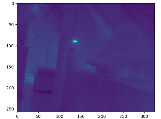
Now it’s possible to collect the valid pixel data, and display it:
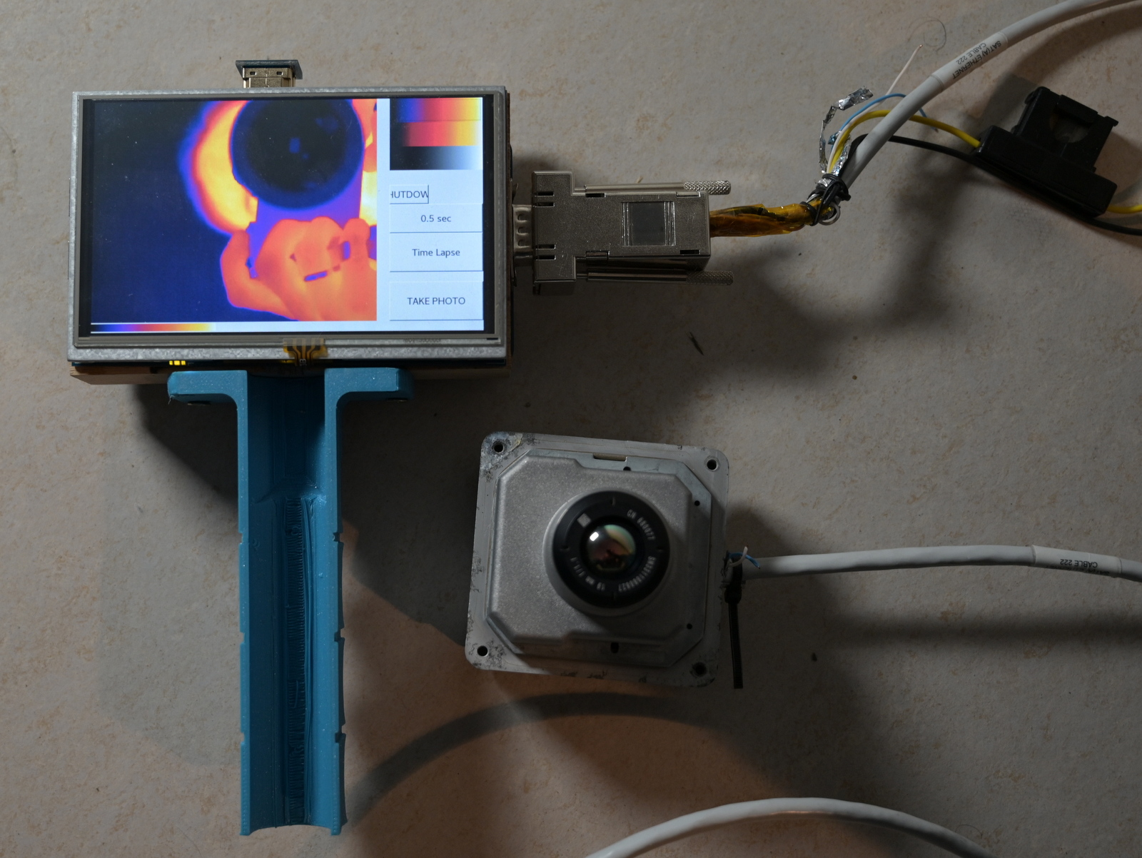
Receiving data in realtime
So far, I’ve received the data using my oscilloscope, but to receive and display it in realtime, a different solution is required.
My plan was this:
- Keep the CAN protocol handling/unlock sequence on some (internal or external) CPU. Don’t bother implementing this in the FPGA for now.
- Deserialize the data.
- Implement the FPD-Link II decoding on the FPGA.
- Potentially do de-packetization (find sync frames, dropping dummy frames) on the FPGA.
- Feed raw 14-bit thermal data into a Raspberry Pi (or whatever).
- Convert to RGB picture.
Deserializing the data
(Link to implementation: Deserializer)
I did this in a very primitive way. I oversampled the raw data rate - 139.7 MBit/s - with 1080 MBit/s (which is the highest supported data rate on the Spartan-6LX9, the FPGA on the OpenVizsla that I wanted to target). This is gives me an oversampling factor of ~7.7x. I use a master/slave ISERDES2 to deserialize this to 8-bit words.
(Link to implementation: Sampler)
The next step is a “bitslip”, i.e. something that can skip or duplicate bits to match the data rate (it does that by shifting and combining two adjacent 8-bit samples into an output 8-bit sample; it can be thought as a sliding 8-bit window that usually increments 8-bit so that each oversampling bit would pass the window once, but can also increment by 7 or 9 bits every once in a while, at which point bits are duplicated or skipped). In this case, to arrive at a plain 8x oversampling rate, I need to increase the rate by ~1/30th, or 1 bit every 3.75 deserialized samples (as each deserialized sample contains 8 bits). I can’t skip a non-integral number of bits of course, but I can balance between skipping every 3th and 4th bits by maintaining a fractional counter (and skip on overflow).
Aside from the coarse rate matching, I need to align the samples to the actual source; ideally oversampling is phase-aligned to the data so that transitions always happen at a specific bit position (since I can’t match the source rate exactly, it will always toggle between two bit positions), so I can sample the bit at the opposite phase (i.e. 4 bits further down).
I do this with a very simple loop that looks for transitions, and if they appear “on the left side”, I know that I’m too fast, so I slow down by bit-slipping into one direction. If they appear on the right side, I’m too slow and I skip an oversampling bit. (In order to improve the response time I actually support slipping two bits in some cases.) Once the transitions happen in the middle, I’m happy and I just keep it running.
Again, this is a very primitive method of clock recovery, but the advantage is that it’s all digital, and can be simulated easily. My standard approach is to get data from an oscilloscope, write a piece of Python code implementing the algorithm in a hardware-compatible way (i.e. no control flow, just cycle-for-cycle processing), and then transition to MiGen - i.e. Python code that creates logic. I would re-write the logic there, simulate it, create debug output that I can compare with the pure software implementation, and verify that it behaves the same.
At the end of all this, I already get an idea of whether I can lock to the data stream or not - if I keep seeing transitions out of phase, I know that I’m not matching the source rate yet. Simulation is great, but to debug realtime signals, it’s great to produce realtime debug output that can be seen on the scope together with the input data.
Decoding FPD-Link II
(Link to implementation: Decoder (FPD-link))
After the data is serialized, I put it into a 28-bit shift registers. I look at the CLK0/1 bits, and if I don’t see them matching, I stop the shift register for a cycle, which shifts the data by one clock. At some point, the CLK0/1 bits will align correctly, and the data is locked.
At this point, I apply the DCB conditional inversion, and the DCA descrambling as described above.
The remaining data is reduced to 16-bit/pixel by removing unused bits, and sent to FTDI for host consumption. The crappy USB controller on the Raspberry Pi can’t handle more than a few Megabytes/s even with a core dedicated to USB communication, so that’s why the data needs to be reduced first by removing redundant bits (which reduces the data rate to 2/3rd).
Displaying Thermal data
To display the data, the 14-bit thermographic data needs to be reduced to a smaller dynamic range. The simplest way is to just re-map min/max to an 8-bit range, and display this as grayscale. That works reasonably well, but more sophisticated algorithms will maintain image details even under a higher dynamic range (for example if the average temperature is pretty cold, and there’s a single, small hot subject, it would squash the majority of the image to just a few bits); an example algorithm that fixes this is histogram equalization, which is relatively easy to implement.
It’s also useful to map the resulting image to a colormap, which helps in amplifying small details. All of this can be easily done on the CPU, though of course it would also be possible to write a fancy shader. It’s hard to do it on the FPGA though because it needs a rather large amount of RAM to store the colormap LUT alone at a decent resolution (10-bit is useful for example, resulting in 24 * 1024 = 24 kbit of data). The histogram equalization also needs a 10-bit table for computing the histogram, at least in a naive implementation. So that’s why I didn’t bother to do this part on the FPGA.
I also added the ability to save raw data into 16-bit PNGs as well as palettized screenshots.
Want your own thermal camera?
First, please note that I can’t share the key that’s required for the UDS unlock sequence. Sorry.
Then, please be aware that there are two versions currently in use - the described NV2 (“2nd Generation”), as well as a newer version called NV3 (“3rd Generation”). The NV3 uses a different host interface - it combines the data and image interface into a bidirectional high-speed interface that’s much harder to interface - and uses an Altera FPGA instead of Xilinx. It also encrypts the firmware. In general, my understanding is that the NV3 isn’t really better, it’s just significantly cheaper to produce and integrate. I haven’t looked much at this camera, and almost nothing of this blog post applies to it (different FPGA, very likely different soft-core, no CAN bus anymore, different physical video interface).
Have fun!