OpenVizsla OV3 - Hardware
Fail.
That’s probably the first word you think of when hearing the word “OpenVizsla”. It all started good in - WTF - 2010 when bushing and pytey thought it would be a good idea to build an open-source USB sniffer.
Scam. That’s what people called the project after unable to provide a working prototype after one year, two years, three years. But let me assure you: this project is not a scam. We just failed. A lot.
I don’t want to swirl up the past - that was done before, but rather present the current state of affairs. TL;DR: It looks good, and OV3 actually a working USB analyzer these days, and it shipped to (almost) all of the original backers. Once all of them shipped, more of them will be sold to the public.
Let’s start with a hardware overview of ov3, the third attempt to get it right. By the way, you can find everything in the openvizsla github repository. Just in case you want to build your own USB analyzer.
Features
Here is what OpenVizsla wants to deliver:
- USB 2.0 High-Speed, Full-Speed and Low-Speed sniffing.
- Full-Rate capture for up to a half-second of full-utilization
- Realtime streaming (assuming reduced utilization) over a USB 2.0 High-Speed host interface
- Fancy software decoding
- Triggering
Since there is no (affordable, at least) silicon that out-of-the-box provides USB sniffing features, the heart of the OpenVizsla is an FPGA. We’re using a Spartan-6 (XC6SLX9) for this purpose, since it’s cheap, fast enough and provides a margin for future improvements.
To buffer, 32 MByte of traditional SDRAM (datasheet, alt) is used; running at 100 Mhz already easily provides enough bandwidth for capturing full-rate USB2.0 High-Speed traffic, but we can likely run it at 133 or 166 MHz if we need to, providing extra bandwidth.
The first two ill-fated incarnations of OpenVizsla used an XMOS microcontroller for the USB host interface. The rationale was that we could do fancy filtering and post-processing. But it turned out that … well, it wasn’t the best idea. In reality the filtering has to happen on an FPGA anyway, since the buffering should happen on filtered data. The XMOS in the end didn’t provide a real advantage. To simplify things, for OV3 we decided to use an old-fashioned FT2232H, which can be used in a FIFO mode (pdf) that allows up to 40MByte/s data transfer over the USB 2.0 host interface. The chip is well-known and we’ve built previous devices for it (twlfpga).
The Board
Let’s take a look at the actual OpenVizsla board:
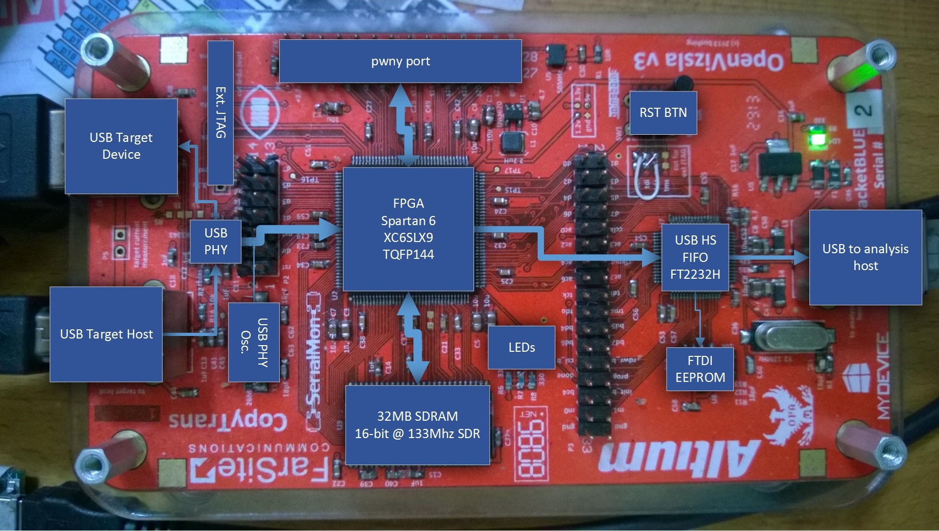
(Note that this is a pre-production version as indicated by the serial number ‘2’. The final version has some bonus features, like SMA trigger input/outputs and doesn’t require the fancy patch wires.)
In the middle there is the mentioned FPGA. Connected directly to it is the
USB PHY (ULPI), which is passively connected to the DP/DM lines between the
Device-under-Test (DUT) USB-A and USB-B connector. The PHY can be put into a
passive sniffing mode, after which the ULPI basically sends a stream with
all received USB data to the FPGA, together with RXCMDs which are special
status reports on out-of-band events like device detection.
The FPGA packetizes the stream, and buffers it in SDRAM. The stream is then sent back to the analysis host via the FT2232H FIFO bridge.
An additional connector brings out a few unused FPGA pins for hacking purposes, and a few more random things like clock sources and voltage regulators make the thing actually work.
All the schematics can be found in the OpenVizsla GIT repository, or as PDF here.
Happy Hacking!